Domiciled at the prestigious science hub of Berlin Adlershof, AEMtec GmbH specialises in the development, industrialization and manufacture of complex micro- and optoelectronic modules and even complete systems. 

to our Jobs

COMPLEX MICRO - AND OPTOELECTRONICS

As an established B2B company for complex and reliable solutions in the field of miniaturization, AEMtec offers a broad technology portfolio including wafer back-end services, chip on board, flip chip, 3D integration and opto packaging.

Customer-specific requirements from the medical, industrial and automation, data and telecommunications, semiconductor and aerospace sectors are reliably implemented soon.

The range of services includes design, development, industrialization, qualification, prototyping (NPI), test and test system development, series production, supply chain management and after sales services

System integration in electronics - challenges and strategies for future packaging technologies

Future technologies such as artificial intelligence, quantum technology or high-performance computing are the basis for solving challenges for society as a whole such as digitalization, the energy transition or environmental issues. At last, this is only possible through advanced or novel system integration strategies in microelectronics and microsystems technology. 

Chiplet technology – Challenges and Opportunities

Optimized performance and integration of various technologies leads to greater efficiency in semiconductor solutions. Chiplet technology is a new design strategy in which, instead of a complex system-on-chip (SoC), several semiconductors (“chiplets”) are connected to each other using very short and dense wiring. 
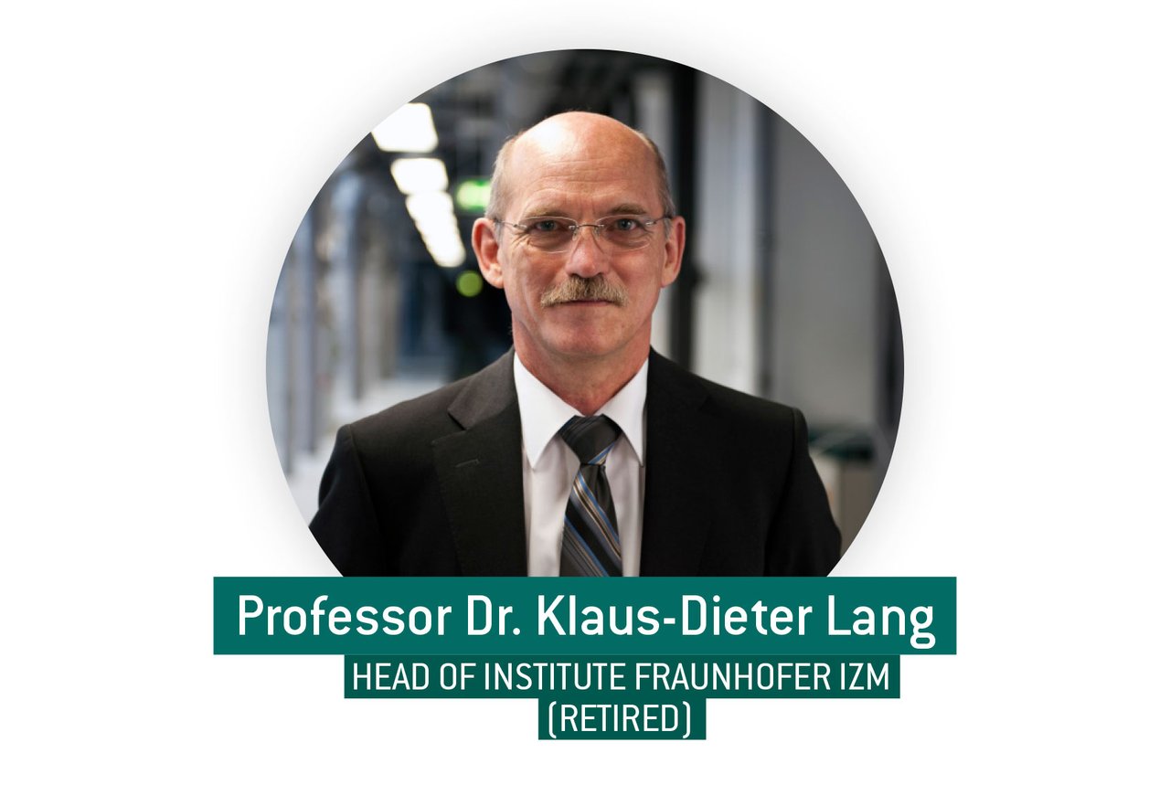
We fully recommend AEMtec as partner for innovative electronic solutions

If you have questions and needs in the field of development, industrialization and manufacturing of complex micro and optoelectronic modules, we recommend AEMtec as reliable and competent service partner.

New UBM equipment in-house

The UBM process is a well experienced part of the wafer back-end services offered by AEMtec. Implementing a new UBM-line, in-house processing will lead to many advantages regarding lead times and quality and create more versatility.


LATEST NEWS

News

News USA

AEMtec and aSpect Systems Join Forces to Expand Technology Portfolio

Berlin, December 20, 2024 – AEMtec GmbH, a global leader in micro and optoelectronics, is pleased to announce the acquisition of aSpect Systems GmbH, a renowned provider of semiconductor testing…

Read more
News

News

WRAPPING UP a successful week at electronica!

Last week, we had the pleasure of exhibiting at electronica, where we engaged in lively discussions with our customers and many new potential partners.

A highlight for us was the keen interest shown…

Read more
News

News

Electoral group meeting - An exciting day in Berlin Adlershof!

On 14.10., the election group meeting of the Chamber of Industry and Commerce took place in the premises of the AEMtec in Berlin Adlershof. Host, Jan Trommershausen, received representatives of…

Read more
News

News

MIKROTECHNOLOGEN GESTALTEN DAS MORGEN!

Herzlich Willkommen im AEMtec Team und viel Erfolg für Eure Ausbildung! Wir freuen uns, dass auch in diesem Jahr vier Auszubildende zum Mikrotechnologen (m/w/d) sich für die AEMtec entschieden haben…

Read more
News

News USA

NEW UBM LINE - next step

A few weeks ago, we shared exciting news about the implementation of our new Electroless Under Bump Metallization (UBM) equipment. It`s time to inform about the next step.

Our new UBM line is now…

Read more
News

News

HIGH SPEED FOR OPTOELECTRONICS

Herzlichen Dank an unsere Teams! Auch in diesem Jahr sind sechs AEMtec-Laufteams für die AEMtec beim Adlershofer Firmenlauf gestartet und setzten sich mit „High Speed for Optoelectronics“ ein.

Read more
News

News USA

Welcome Ingolf @ AEMtec USA

Exciting news! Ingolf Schlosser has just arrived in Boston and will be starting at our US Tech Center as Head of Engineering. 

With longstanding engineering experience and a history of tackling…

Read more
News

News

ALSO, IN THE AEMtec PORTFOLIO: X-RAY INSPECTION!

WHAT IS X-RAY INSPECTION?

X-Ray Inspection technology is a non-destructive testing method used to analyze the internal structure of objects without causing any damage. It utilizes X-rays to capture…

Read more
News

News

Congratulations!

Congratulations to Josi and Erik on successfully completing their training as microtechnologists (m/f/d).

We are delighted for you and are also very pleased that you are staying with us and joining…

Read more
News

News

GOING FOR CO2 NEUTRALITY

As the AEMtec team, we believe that environmental protection is essential and have therefore adopted eco-friendly policies.

Our dedicated and specifically qualified colleagues in environmental…

Read more
 

Markets

PARTNER

Stable network for sustainable success

AEMtec maintains a strong network with prestigious institutes from the worlds of science and industry, ensuring the application of cutting-edge research into processes and high-end technologies.