UBM Electroless Ni-Au Plating
- Incoming Inspection
- Setup
- Continuous monitoring of chemical baths
- UBM
- Process inspection
Balling, Ball/Bump Forming
- Flux/Paste Printing
- Application of solder balls
- Solder ball repair
- Reflow soldering
- Wet cleaning
- 2D-Inspection
- e-Wafermap update
Testing Wafer
Associated services:
We also perform Wafer Testing and Grinding process in cooperation with our partners, under the responsibility and control of AEMtec.
Grinding Wafer, Si, Glass, etc.
Associated services:
We also perform Wafer Testing and Grinding process in cooperation with our partners, under the responsibility and control of AEMtec.
Wafer Dicing or MEMS
- Incoming Inspection
- Lamination of Wafer
- Wafer dicing
- Process Inspection
Assembly, FC, WLP, CoB, CoG
- Flip Chip
- Soldering
- SMT
- Test
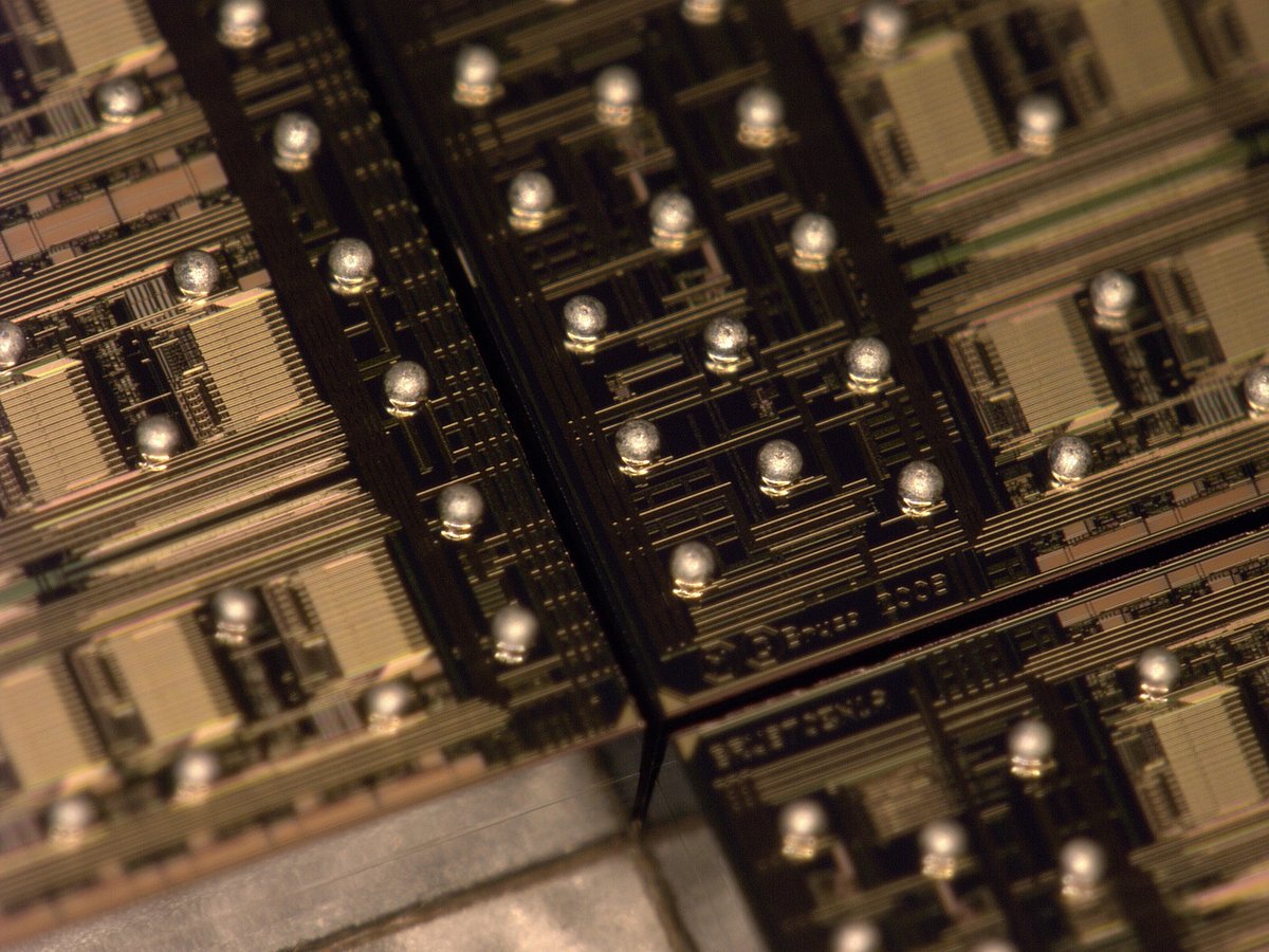
Application of the UBM is performed via an electroless plating process, a technology developed by Fraunhofer IZM. The contacts are made chemically by deposition of nickel and gold. UBM for solder contacts or nickel bumps can be generated for flip chip bonding. The entire process is performed without individual masks. This reduces cost and accelerates the production process.
- Wafer Thickness: > 200µm
- Pad-Metallization: Al or Cu
- Bump-Metallization: NiAu, NiPdAu, typical bump height 5µm or 20µm
Target Application: UBM for Solder Ball or Bump Mounting, ENB for ACA, ICA or ACF bonding
AEMtec uses fully automated systems for the application of solder balls by ball drop or printing at wafer level. Wafer from 6 to 12 inch with a solder ball diameter between 50 and 400 µm in every available alloy can be processed. Part of the system is a fully automated AOI and repair of the solder balls. This guarantees a consistently high yield with a very limited process time, and reliable positioning even with the smallest ball diameters.
- TARGET APPLICATION: Flip Chip, Wafer Level Packages
- Wafer Thickness: > 200µm
Fully automated precisions saws cut the wafer. The device can be used for processing substrates such as silicon, glass, ceramic, SiC and other structures up to 300mm (12 inches) in size. Processing is fully automated, from the cassette feed to positioning and sawing and on to cleanup and replacement into the cassette, all at the push of a button. An automated water treatment facility ensures full compliance with environmental regulations.