Benefits
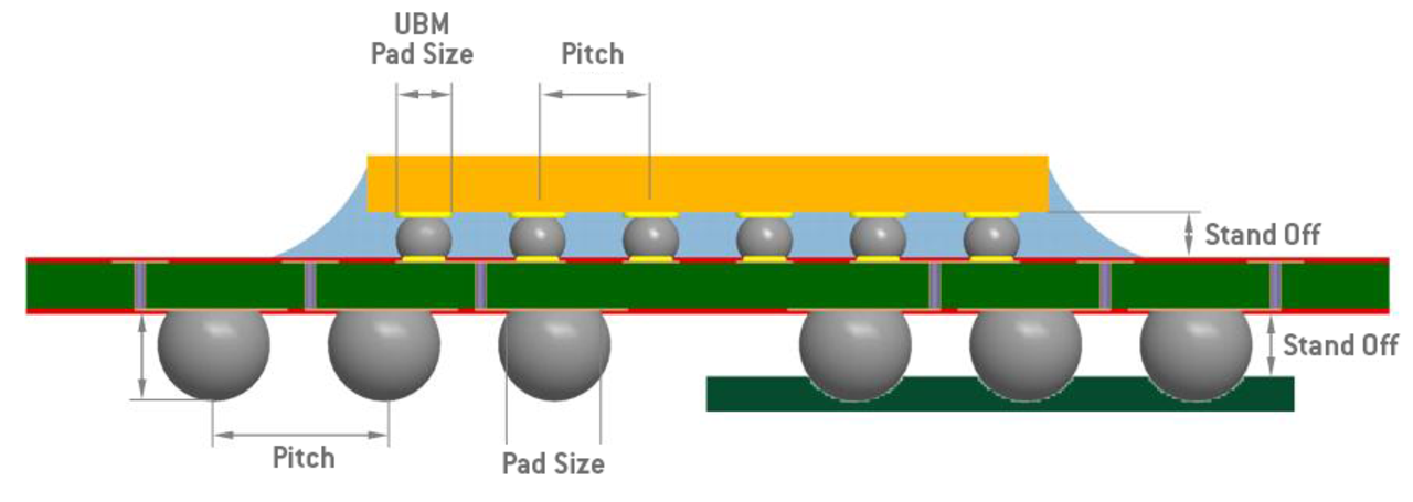
The shortest possible conductor paths are vital, especially for high-frequency applications. The benefit of the flip chip method is that it delivers maximum packing density with low space requirements.
When the active surface of a component is required on the top side, but the connection needs to be executed like in the FC method, AEMtec can use the through silicon via method (TSV) to develop the required solution. AEMtec has successfully used TSV components for years.
Flip Chip Technologies
- Flip chip soldering – up to 180 µm pitch
- Isotropic bonding (ICA) – up to 800 µm pitch
- Anisotropic bonding (ACA) – up to 50 µm pitch
- Nonconductive bonding (NCA) – up to 80 µm pitch
- Ultrasonic – 100 stud balls at max.
- Thermocompression – number of bumps depends on the size
- Anisotropic adhesive film (ACF) – 50 µm pitch

